OpenGL-Compliant GPU on FPGA
Post is under construction
About
A fully-functional, OpenGL-compliant graphics processor (SGP) using an FPGA-based platform. I implemented the 3D rendering pipeline, graphics drivers, and OpenGL test applications. This project showcases my ability to do hardware and software design, and analyze and optimize performance between graphics applications, drivers, and hardware architecture.
Development Environment: AMD Xilinx Vivado
- Used for developing, simulating, and loading FPGA designs
Target Platform: Digilent Nexys-Video FPGA
- Communication to deployment platform using USB serial UART and gigabit Ethernet interfaces
Overview:
- Implemented all stages of the 3D rendering pipeline in VHDL
- i.e. vertex fetch, primitive assembly, vertex shader, rasterization, fragment shader, and color blending
- System tested GPU drivers and hardware logic with C++ OpenGL applications
- Designed vertex and fragment shader cores to execute GLSL instructions on the GPU
- Implemented high-performance rasterization algorithms to reduce traversal and interpolation time and hardware resource consumption
- Analyzed AXI signal waveforms for integration testing by leveraging System Integrated Logic Analyzer (ILA) cores
- Compared scripted test results to hand calculations
- Managed data flow from custom OpenGL drivers to the GPU using direct memory access (DMA)
OpenGL Drivers
In order to effectively test OpenGL application on the FPGA, OpenGL calls are executed on both the FPGA and the workstation graphics card simultaneously. Any OpenGL application that can run on the workstation can use the SGP with little t\o no software changes. The figure below shows a diagram of the library structure to support this feature.
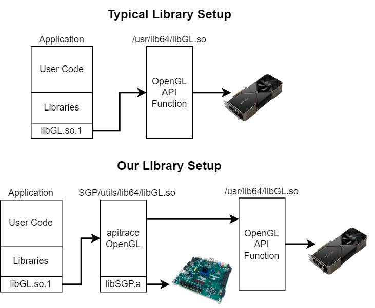
The open source project, apitrace, was utilized to intercept and pass all OpenGL API calls to both devices. It was trimmed down and heavily modified to support transferring data to the SGP.
System Diagram
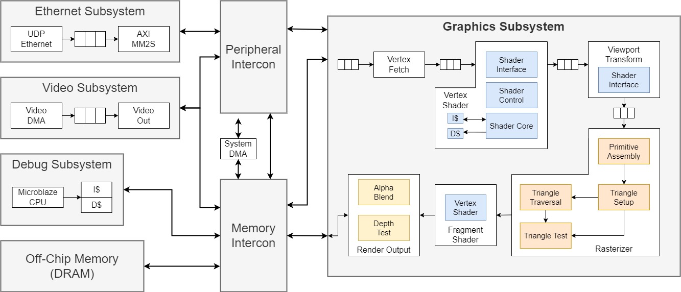
System Diagram Notes
Data arrives via the Ethernet Subsystem, which uses the AXI bus information encoded in each packet to create AXI requests, which it directly connects to the primary interconnect fabric in the design (Peripheral Intercon in the figure)
The Video Subsystem is responsible for reading buffer data from off-chip memory (via the Video DMA component) and transmitting this data out over HDMI (via the Video Out component).
The Debug Subsystem allows us to bypass sending data over Ethernet and can directly access all other components in the system. It does this via a Xilinx-provided Microblaze core, which is a small CPU similar to the pipelined processor I made.
The Graphics Subsystem has an input queue for receiving incoming vertex data, and can be configured to perform different tasks such as depth & alpha testing.
The Memory Interconnect multiplexes requests coming from all the different components, and sends them to off-chip memory. Separate DMA modules allow for offloading larger read/write transactions while minimizing off-chip and on-chip overhead.
Each component has a corresponding entry in a global memory map with offsets for configuring registers. The Nexys-Video FPGA board has 512 MB of DRAM memory, and a set of addresses are reserved for off-chip memory.
Acronyms
- AXI Memory Mapped to Stream Mapper (AXI MM2S)
- Used in pairs to communicate between blocks. The interface is memory mapped on both ends.
- Instruction Cache (I$)
- Data Cache (D$)
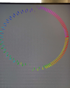
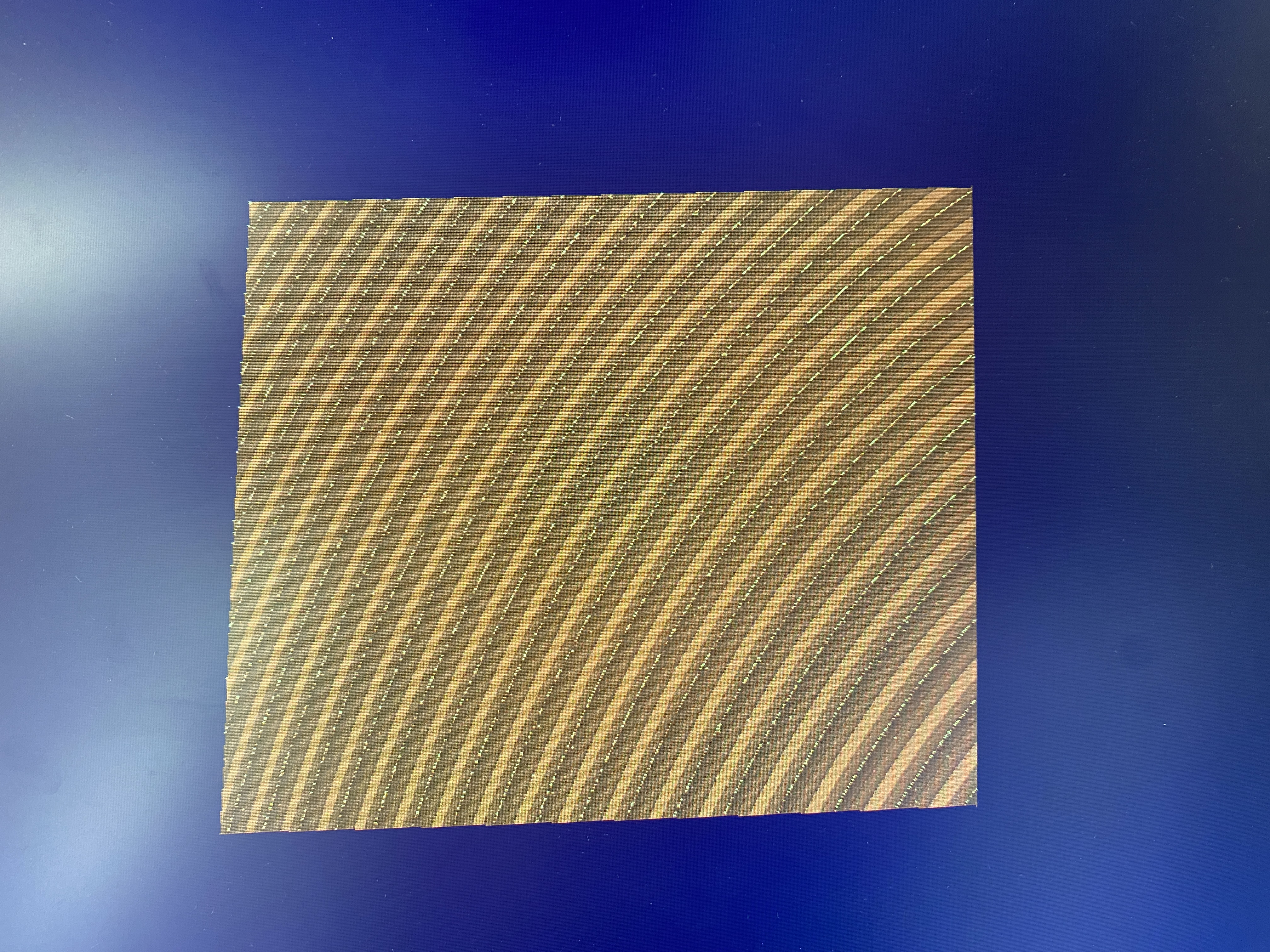
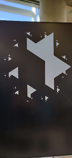
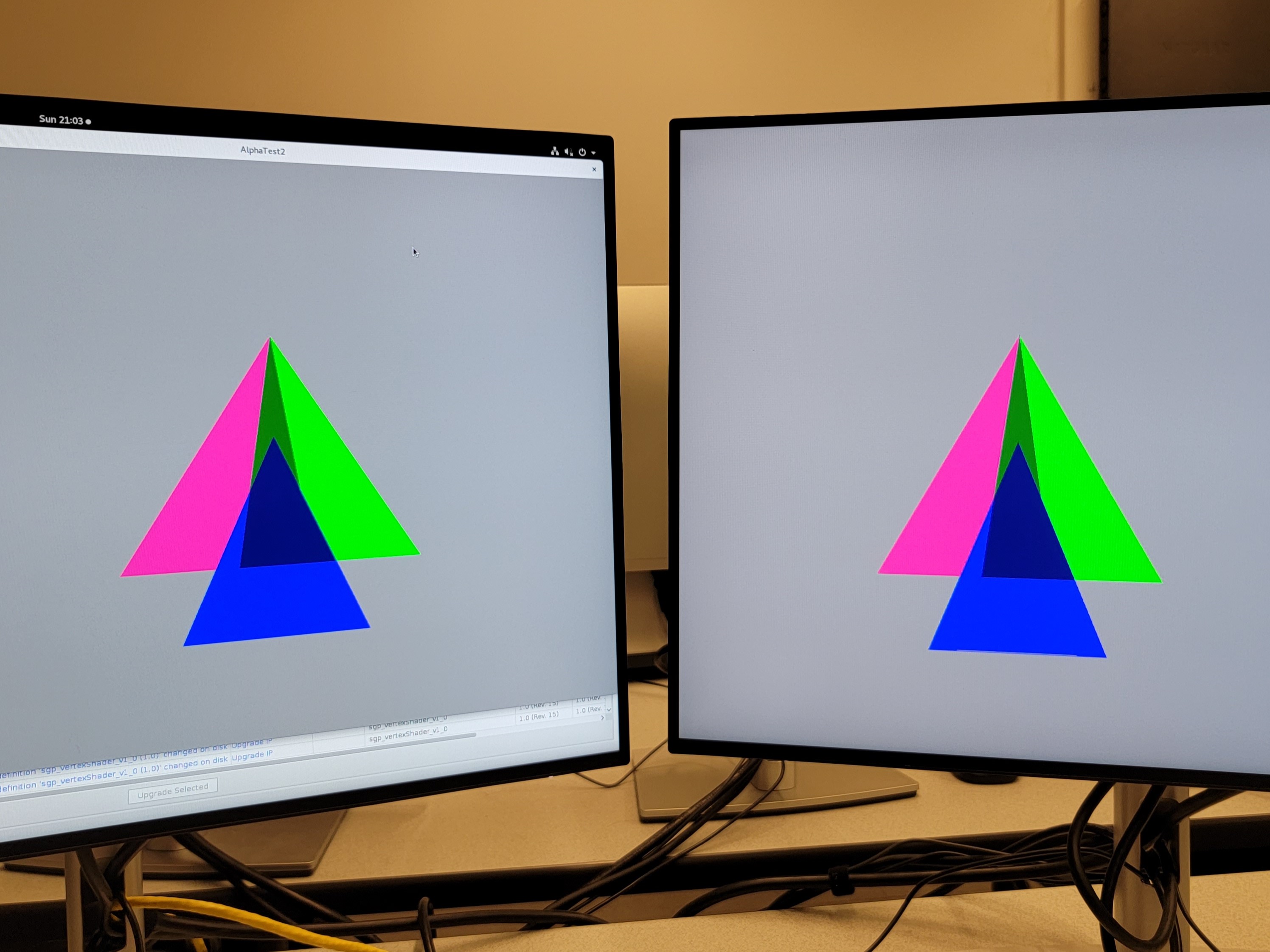
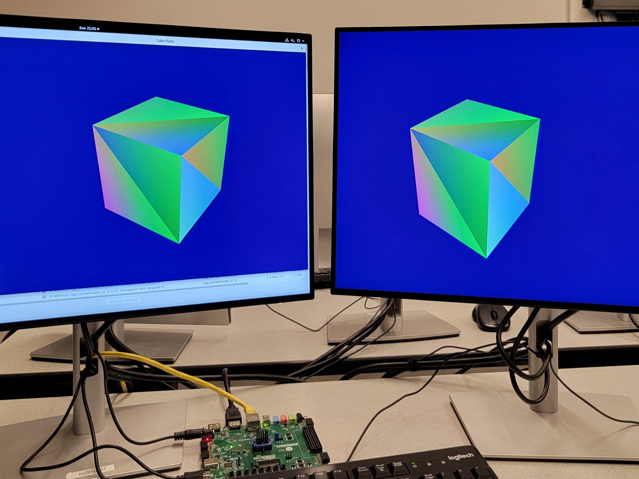
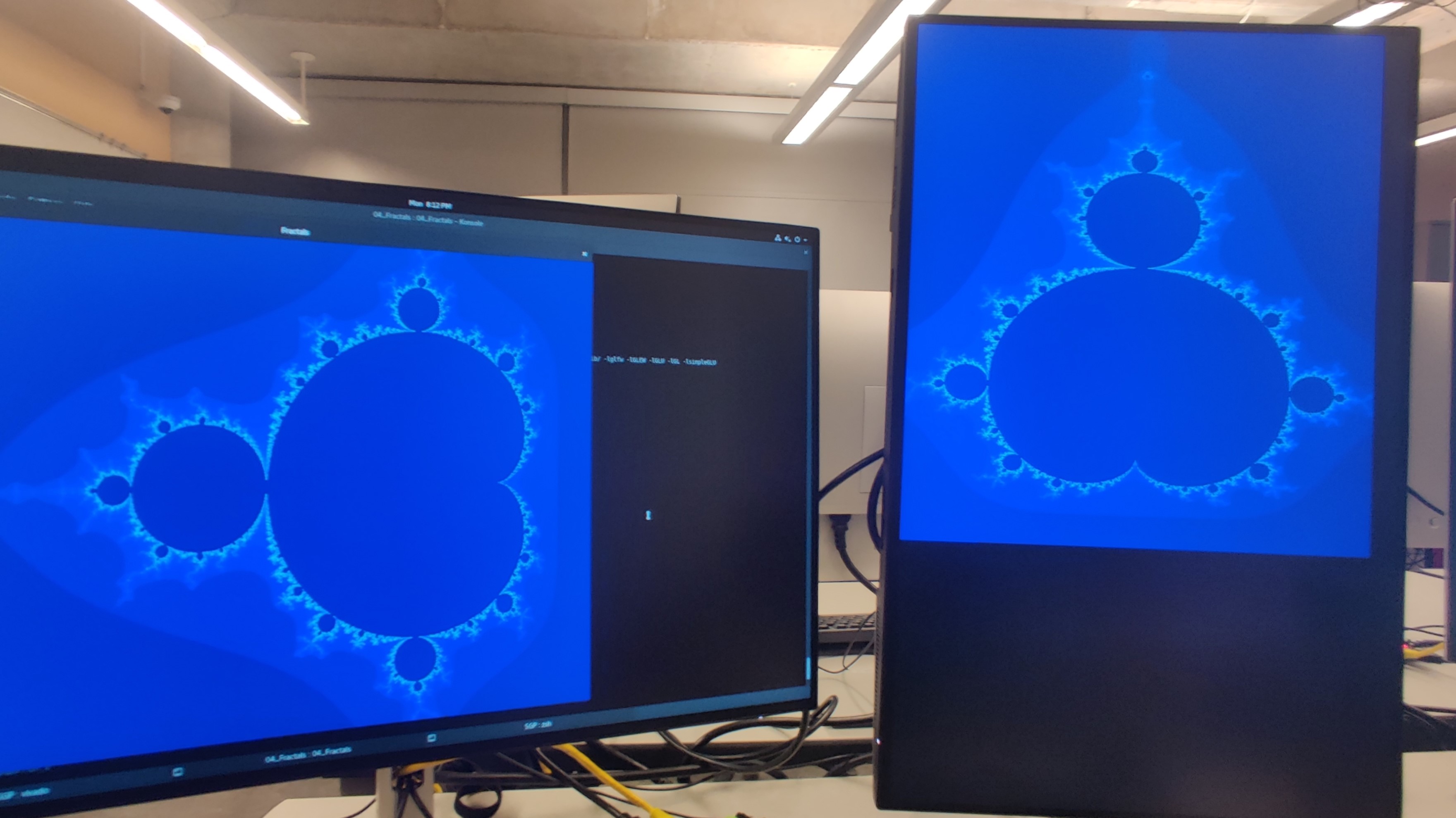
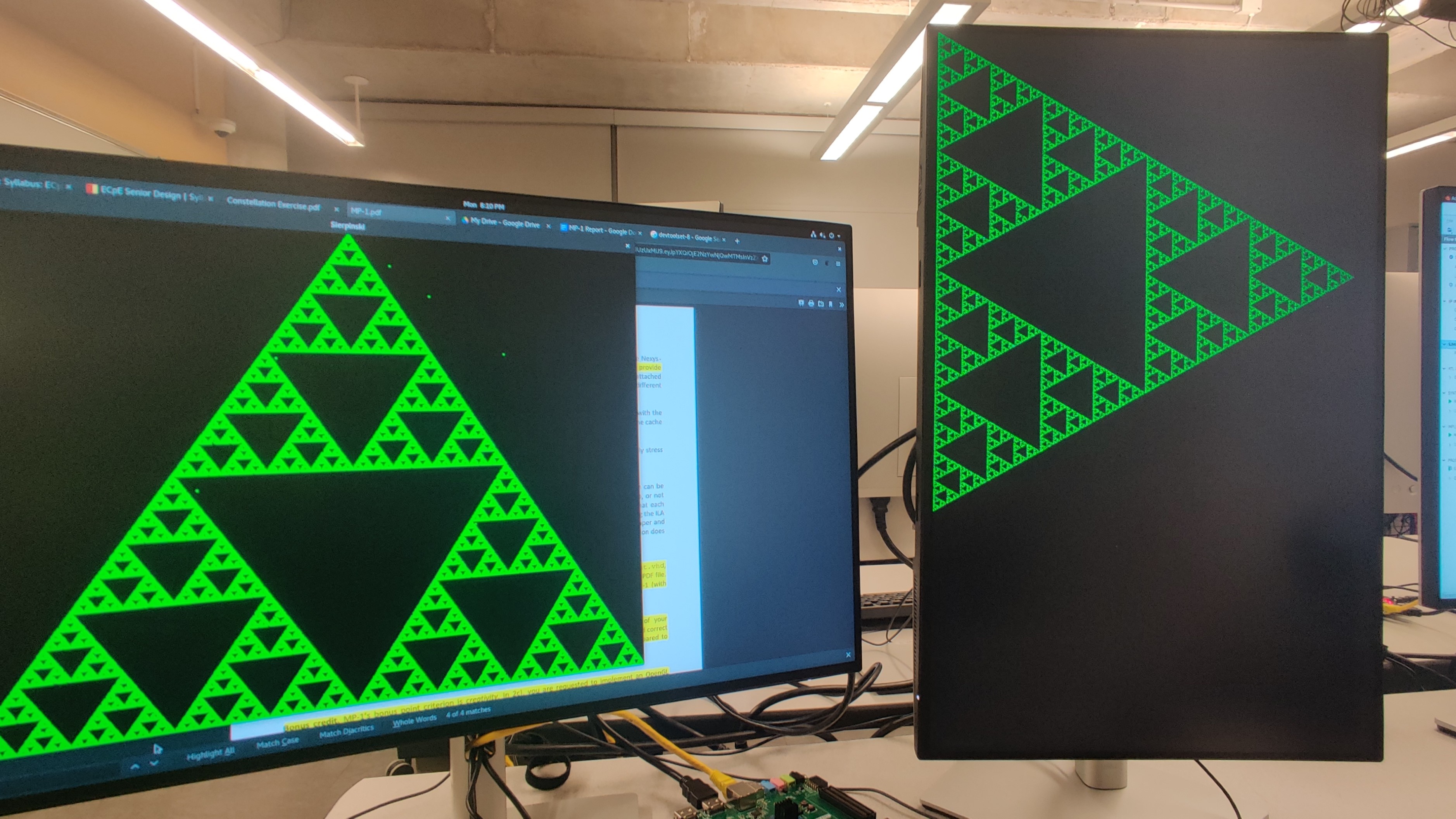
Test Applications
Several test applications were created to test full or individual systems in the SGP. The following images are output from the FPGA.

Fun Bugs