MIPS Processor (Technical)
This is a technical description of my MIPS processor project. To read from a non-technical perspective, check out MIPS Processor (Non-Technical).
WIP
About
This write-up showcases an in depth exploration of three different processor designs: a single-cycle design, a software-scheduled pipeline, and a hardware-scheduled pipeline. Each processor underwent careful design, implementation, and performance analysis, highlighting the practical applications and tradeoffs involved in computer architecture.
The primary objective was to create functioning MIPS assembly processors with schematic designs, control spreadsheets, and VHDL implementation. The single-cycle processor, built first, introduced us to novel concepts in computer architecture design. The design, components, and tests were all created from scratch, and subsequent processors based on the single-cycle design aimed to optimize performance through pipeline strategies and hazard mitigation.
A set of test benches were compiled in order to determine the performance of each of the three processor designs. Each one demonstrates a set of advantages and disadvantages that must be considered when choosing one implementation over another.
View the source code
2 Instruction Set
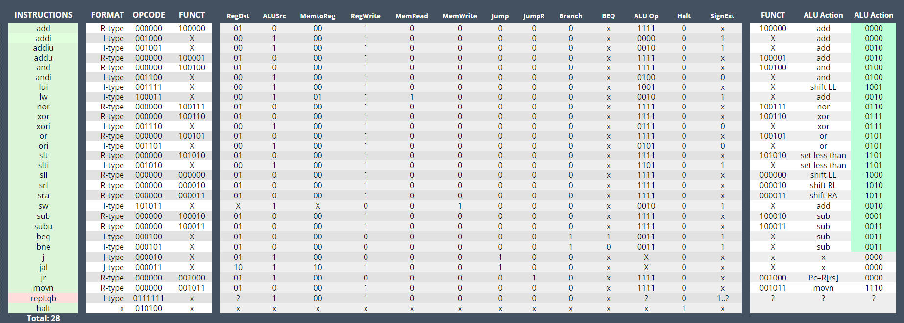
These processors support a limited MIPS instruction set seen below.
Produce: Change registers or memory
Consume: Access registers or memory

Control Logic
Each instruction was broken down into the required signals to operate correctly.
3 Single-Cycle Processor
3.1 Design
This processor is a single-cycle design that aims to perform one instruction in just one cycle of the CPU. There are several advantages and disadvantages of a design like this. The design is rather straightforward, but because the cycle time is fixed to the slowest instruction, faster instructions cannot execute more quickly.
3.2 Benchmarks
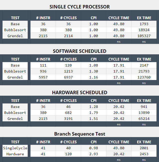
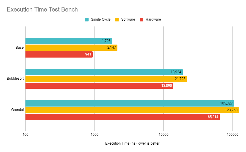
As expected, the single-cycle design executes each test in the same amount of cycles as there are instructions, resulting in a CPI of one. The cycle time however showcases that the critical path of the processor is 49.80ns.
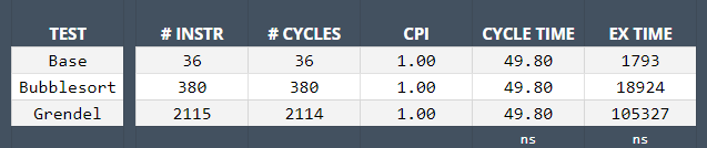
| Test | # Instr | # Cycles | CPI | Cycle Time | Ex Time |
|---|---|---|---|---|---|
| Base | 36 | 36 | 1.00 | 49.80 | 1,793 |
| Bubblesort | 380 | 380 | 1.00 | 49.80 | 18,924 |
| Grendel | 2,115 | 2,114 | 1.00 | 49.80 | 105,327 |
| ns | ns |
3.3 HW Optimization
Since the CPI can’t be improved, other factors have to be considered for optimization. In particular, the cycle time is limited by the critical path of the processor. The critical path of this processor is through the ALU. Since the processor’s cycle time is bound to the latency of the critical path, optimizing the ALU would directly improve the performance.
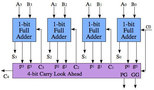
In its current form, the ALU uses a simple ripple carry adder that is the slowest component outside of memory access. The latency comes from the propagation delay of the carry bits, as one adder can’t compute until the previous adder’s carry bit is produced.

A carry-lookahead adder solves this problem by computing whether a carry will be generated before it actually computes the sum. Below is an example of one design, although the benefits are only seen for larger computations. This would significantly decrease the latency of the ALU and improve the critical path of the processor. A lookahead adder would significantly decrease the latency of the ALU and improve the critical path of the processor, but would increase the area and power required.
4 Software Scheduled Pipeline Processor
4.1 Design
The software scheduled pipeline processor design naively implements a pipeline design without any hazard mitigation. The pipeline features five stages: Instruction Fetch, Instruction Decode, Execute, Memory, and Write Back.
4.3 Benchmarks
As expected, the number of instructions are increased because hazard mitigation has to be completed in software using nops. Because of the pipelined design, however, the CPI manages to stay relatively close to one. The cycle time is also improved due to the critical path only being between two pipeline registers rather than end-to-end. So far it looks good, except when we begin to look at the overall execution time. Even though the CPI is close to one, we have increased the number of instructions and cycles to complete the test programs significantly.
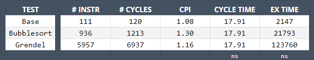
| Test | # Instr | # Cycles | CPI | Cycle Time | Ex Time |
|---|---|---|---|---|---|
| Base | 111 | 120 | 1.08 | 17.91 | 2,147 |
| Bubblesort | 936 | 1213 | 1.30 | 17.91 | 21,793 |
| Grendel | 5,957 | 6,937 | 1.16 | 17.91 | 123,760 |
| ns | ns |
4.2 HW Optimization
The critical path of this processor design is the execution stage, which includes the ALU. Similar to the previous design, a carry lookahead adder would improve the performance of the ALU thus decreasing the cycle time. Other logic in this stage can be moved to adjacent stages where possible as well.
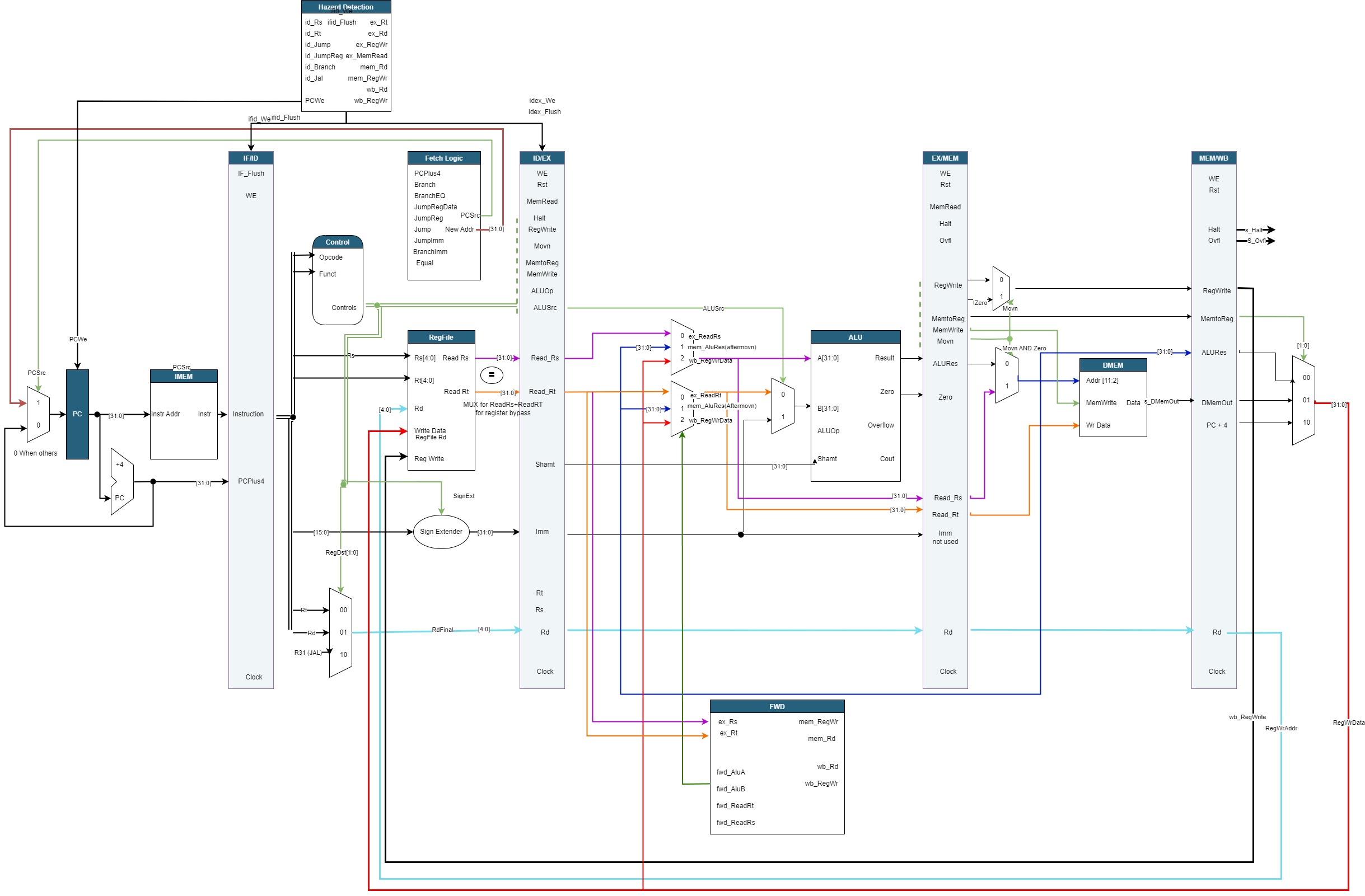
5 Hardware Scheduled Pipeline Processor
5.1 Design
The hardware scheduled pipeline processor features the same 5 stages as the software scheduled variant with the addition of hazard mitigation techniques. The purpose of automatic stalling and forwarding improves the performance of the processor by decreasing the number of wasted cycles that the software-scheduled design saw by inserting nops. The hazard detection component inserts stalls and the forwarding component forwards data around
5.1.1 Design Diagram
5.1.2 Data Hazard Avoidance

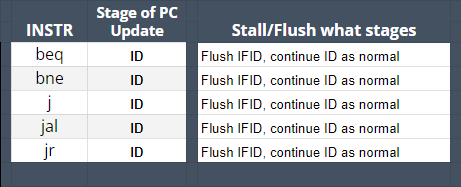
5.1.3 Control Hazard Avoidance
5.2 HW Optimization
5.3 Benchmarks
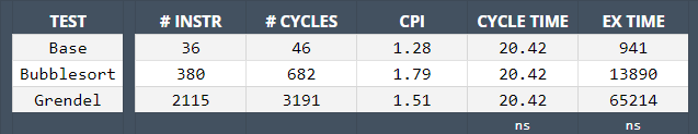
| Test | # Instr | # Cycles | CPI | Cycle Time | Ex Time |
|---|---|---|---|---|---|
| Base | 36 | 46 | 1.28 | 20.42 | 941 |
| Bubblesort | 380 | 682 | 1.79 | 20.42 | 13,890 |
| Grendel | 2,115 | 3,191 | 1.51 | 20.42 | 65,214 |
| ns | ns |
6 Software Optimization
7 Analysis
7.1 Execution Times
7.2 Branch Sequence Test
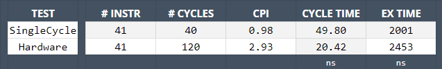
| Test | # Instr | # Cycles | CPI | Cycle Time | Ex Time |
|---|---|---|---|---|---|
| SingleCycle | 41 | 40 | 0.98 | 49.80 | 2,001 |
| Hardware | 41 | 120 | 2.93 | 20.42 | 2,453 |
| ns | ns |